- Our Solutions
INNOVATIVE SILICON PHOTONICS SOLUTIONS FOR TOMORROW'S TECHNOLOGY
Silicon Photonics
We provide enhanced foundry services for silicon photonics through a dedicated 8” commercial fab with intellectual property (IP) and know-how to convert customer design into reality.
Silicon Photonics Foundry Services
At CompoundTek, we transform customer designs into high-performance silicon photonic products through our proprietary manufacturing process and dedicated 8” CMOS foundry (90nm-180nm).
Why Choose CompoundTek?
- Advanced fabrication – A production-proven 8” commercial fab with exclusive IP & expertise to bring your designs to life.
- Fast turnaround – Full reticle field or Multi-Project Wafer (MPW) runs delivered in under 2 months, depending on mask layers.
- Scalable production – Supporting both rapid prototyping and high-volume mass production for seamless scalability.
Partner with us to accelerate your silicon photonics innovation.
Our Technology
Silicon photonics is revolutionizing data communications, enabling faster and more efficient interconnects for 100Gbe, 400Gbe, 800Gbe, and beyond. With growing demands from data centers and fibre-to-the-home (FTTH), advanced functionalities like wavelength tuning and switching are becoming essential.
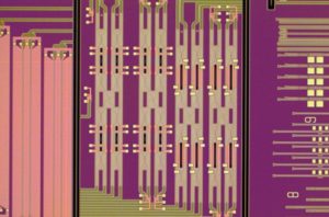
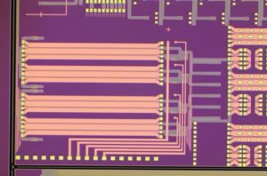
CompoundTek provides a production-proven platform for fabricating silicon photonic ICs, offering a robust Process Design Kit (PDK) and essential building blocks for Multi-Project Wafer (MPW) and standalone product runs. Our technology supports applications such as biomedical sensing, LIDAR, optical interconnectivity, AI/ML, and high-performance computing.
Key features include:
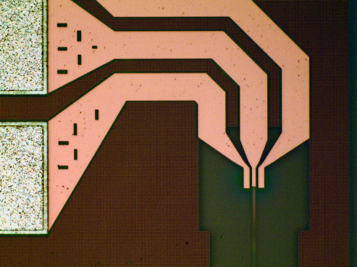
- Precision Si & SiN Waveguides – High-performance optical pathways for maximum efficiency
- Thermal Tuning – TiN & ion-implanted heaters for precise wavelength control •Advanced Ion Implantations – Six doping options (N, N+, N++, P, P+, P++) for optimized performance
- Ge Photodetectors – Lateral & vertical designs for superior detection
- Robust Metal Layers – Ultra-thick Cu & Al for high-reliability interconnects
- Advanced Etching Techniques – Deep trench silicon & oxide etching for tailored optical components
CompoundTek empowers innovators to push the boundaries of silicon photonics.
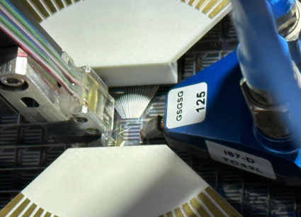
World’s first Agnostics and Dedicated Silicon Photonics (SiPh) Test Hub with vertical and edge optical coupling
Located in Singapore, the state-of-the-art SiPh testing services hub caters to the rapidly evolving demand in the development of SiPh industry. The facility focuses on SiPh on-wafer testing, housing state-of-the-art equipment, instrument controls and test methodologies that are custom-built by CompoundTek and its technology partners.